Transmission Electron Microscopy (TEM) and related techniques enable theimaging (2D or 3D) and atomic-scalestructural and chemical analysis of very thin samples.
Where an optical microscope uses a beam of light and glass lenses, electron microscopes usea beam of electrons and magnetic lenses. The much shorter wavelength of electrons enables electron microscopes to offer far greater resolution.
In transmission electron microscopy, the electron beam passes through the sample at high speed. The interaction between the electrons and the sample produces radiation that is transcribed into an image that can be viewed on a screen.
MET microscopy equipment
Nant’Themis
Contact and prices
For access to MET microscopy equipment and prices, please contact us by email :
These microscopes are also part of the Groupement d’Intérêt Scientifique CIMEN (Centre Interdisciplinaire de Microscopie Électronique de Nantes).
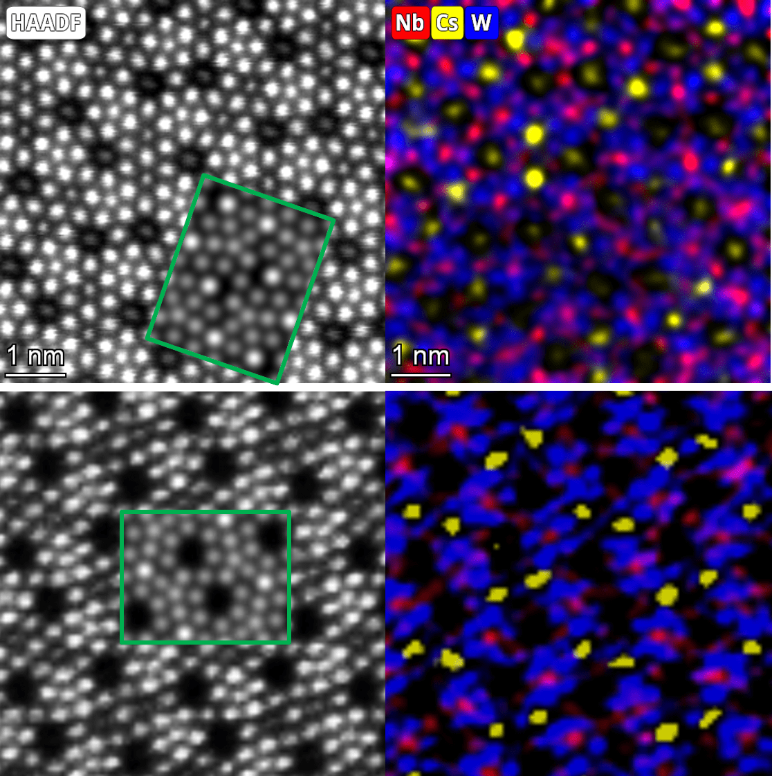
Collaboration with Prof. Bruce Dunn’s team (University of California, Los Angeles) to develop fast-charging battery materials. MET microscopy enables structural hypotheses obtained on a larger scale to be validated at the atomic scale.
Examples and applications
“By way of comparison, it’s so powerful that it could be used to analyze what a tennis ball is made of on the Moon… from Earth! This is a real technological breakthrough in the world of microscopy, opening up new prospects for knowledge and innovation.”
To accelerate the use of electric vehicles, it is essential that batteries can be recharged in a matter of minutes with no loss of capacity. One solution is to replace the negative graphite electrodes used in Li-ion batteries with materials based on transition metal oxides.
In this study, the hexagonal tungsten bronze Cs0.5Nb2.5W2.5O14 and its protonated derivative were characterized by TEM. High-resolution STEM images and associated atomic-scale mappings revealed that :
half of the Cs cations are extracted from the Cs0.5Nb2.5W2.5O14 structure, mainly in the heptagonal channels, to form the compound H0.25Cs0.25Nb2.5W2.5O14
This translates macroscopically into a higher specific capacity of the protonated material compared to its equivalent prior to ion exchange.