Scanning electron microscopy (SEM) enables us to produce images of the surface of a sample, with a magnification of up to 1,000,000 times and a resolution in the nanometer range.
The SEM uses an electron beam to scan the surface of a sample point by point. The electron-matter interaction then generates different emissions (electrons and photons), collected by detectors and used to create an image of the sample surface.
SEM is also very useful for associated peripheral techniques, such as energy dispersive spectroscopy (EDS), which provides information on the chemical elements present in the sample and their respective masses.
With its dual ion and electron column, the SEM/FIB (Focused Ion Beam) enables the sample to be observed by conventional scanning electron microscopy and/or to be subjected to ion beam abrasion (machining of the sample surface), in particular for the preparation of thin plates which will then be characterized by TEM microscopy.
Our Scanning Electron Microscopy equipment
SEM/FIB Zeiss Crossbeam 550L
MEB FEG JEOL JSM 7600F
MEB JEOL IT510
FEG Zeiss Merlin SEM
Zeiss Leo 1450VP SEM
Keyence VHX 2000 digital microscope
Zeiss Axio Imager optical microscope
Contact and prices
For access to SEM microscopy equipment and prices, please contact us by email :
The SEM/FIB is part of the Groupement d’Intérêt Scientifique CIMEN (Centre Interdisciplinaire de Microscopie Electronique de Nantes).
Nantes-based research organizations Arc’Antique, Mines-Télécoms and the Laboratoire de Planétologie took part in the project to renew the EDS analysis-oriented SEM at the Lombarderie site. They are among the entities that regularly use PLASSMAT electron microscopes, including CEISAM, ISOMer and SUBATECH.
Collaboration with the RMeS laboratory (Regenerative Medicine and Skeleton Laboratory) to develop methods for 3D visualization of biomaterials for bone regeneration (FIB and SEM under cryogenic conditions).
Examples and applications
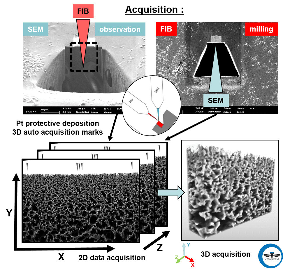
Example of a 3D SEM/FIB study
The valorization of microalgae involves a filtration stage to separate the biomolecules for different uses, ranging from food supplements to green fuels, cosmetics and pharmaceuticals. The performance of the membranes is essential in this process, as they must not become clogged with the filtered products.
Characterization of polymer membranes using 3D FIB acquisition enables us to detail pore structure and the behavior of filtered products in their structure, by visualizing the interior of the material they are made of. To achieve this, the FIB ion beam successively abrades a large number of layers of the material, while the electron beam images these layers as the abrasion proceeds. The result is a stack of images which, when reassembled by software, provides a 3D view of the volume explored, enabling dimensional measurements of porosity.
Joining thick parts by welding generates undesirable deformations and stresses. This has an impact on the service life of the assembly, as well as on its quality. The electron backscatter diffraction (EBSD) technique was used to characterize the weld microstructure after the use of different stainless steel filler metal mixtures whose different coefficients of expansion may enhance the defects studied. The maps obtained showed the effectiveness of a three-phase mixture (austenite, ferrite and martensite) in reducing undesirable deformations by 67%.
Example of an EDS study with the 5800LV: EDS mapping
The recycling of radioisotopes of iodine, a highly volatile element, has not yet been mastered. One solution appears to be immobilization in a glass-ceramic under high-pressure conditions. The 5800LV was used to characterize the solutions tested at the Laboratoire de Planétologie et Géosciences de Nantes in order to highlight the different chemical phases present, after coating and polishing the samples. The EDS detector was used to carry out elemental mapping of chemical elements, highlighting the existence and distribution in the glass of iodinated chemical compounds that could present a potential solution to the problem.